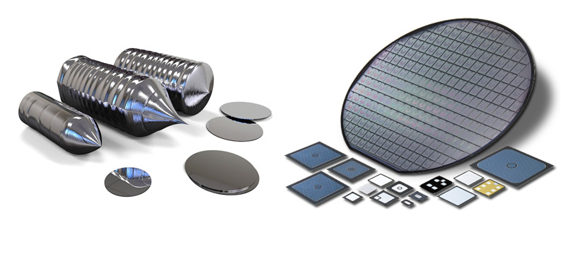
A wafer is a thin slice of semiconductor material used to fabricate integrated circuits or other microdevices1. Also called a slice or substrate, wafers must undergo a number of steps in the preparation process before they are ready for use.
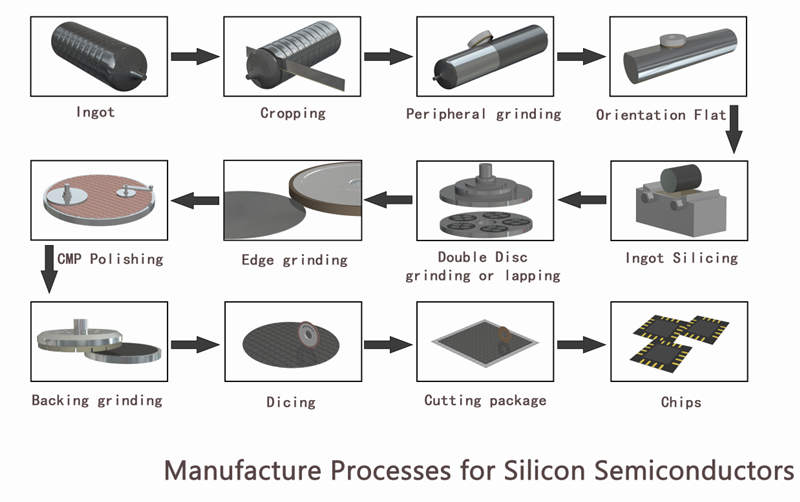
Manufacturing processes for silicon semiconductor
Silicon Ingot ⇒ Cropping(electroplated bandsaw) ⇒ Cylindrical / Flat Grinding Silicon Rod ⇒ Ingot Silicon (diamond wire) ⇒ Lapping (double side wheel/polishing pad) ⇒ Edge Grinding ⇒ Surface grinding ⇒ polishing⇒ wafer⇒ patterning ⇒ back grinding (vitrified / resin wheels) ⇒ dicing (dicing blades)⇒ chips ⇒ molding ⇒ packaging
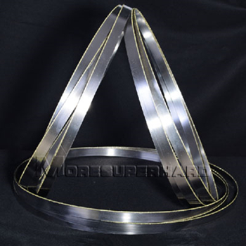
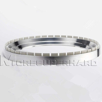
Cutting silicon ingot in semiconductor industry. Thery are also cut sapphire ingot , quartz glass, et
cEdge shapes diamond bandsaw blades: continuous, segmented ( half moon) and serrated shape
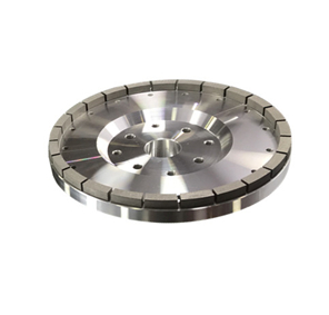
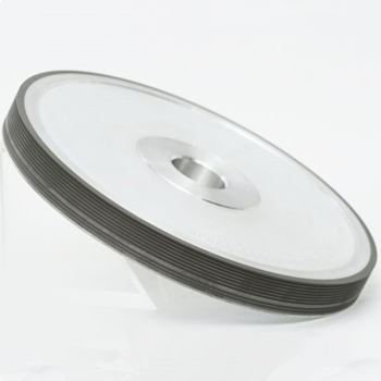
► Cylindical / Surface Grinding Wheels
Peripheral grinding of silicon ingots, or processing the outer surface of silicon ingots and to make orientation flatBack grinding wheels are used for the thinning and fine grinding of the silicon wafer.
► Dicing Blades ( Hub type and Hubless type) 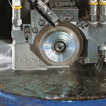
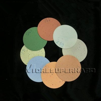
Polishing and finishing of glass, LCD/LED substrates, precision optics, hard disk, metal and semiconductor wafer surfaces


